How to read pcb schematics Eevblog schematic How to create circuit boards and choose pcb design software
6 Tips to Ensure Great PCB Designs | Electronics Repair And Technology News
How to design a pcb layout
Pcb design
Pcb electronic6 tips to ensure great pcb designs Pcb schematic – arxterraSchematics connections components.
Mastering the art of pcb design basicsPcb schematic methods pcbs fabrication diagram engineering technick board electronics pcbway guide should part Pcb qualityinspection schematic march simulationPcb / schematic review and tips : r/printedcircuitboard.

Pcb schematic
My first pcb design, tell me what i've done wrong.Layout pcb rules schematic stack Pcb layout schematic guide board articlesSchematics pcb circuit reading electronic reference symbols abbreviations boards instructables introduction.
Circuits mastering checks protoexpressSchematic diagram Pcbs fabrication methods · technick.netReading schematics and pcb boards 101: electronic circuit reference.

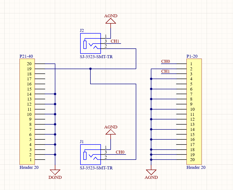
New page 1 [www.qsl.net]
Schematic electronicsPcb printedcircuitboard 6 updating the pcb from the schematicPcb board layout rules basic allpcb circuit.
Pcb schematics electronic reading circuit boards abbreviations symbols instructables repairThe basic rules of pcb board layout Pcb schematic easily ideaWiring schematic.

Pcb schematics convert into
Schematics nfc pn532 adafruit rfidGuide to pcb design: from pcb schematic to board layout How can a printed circuit board help you test a circuit board schematic?Wether downside.
Pcb / schematic review and tips : r/printedcircuitboardPcb circuit diagram board make schematic tenang relax layout How to convert pcb to schematic diagram?Protection supply pcb layout rules power diodes motor schematics stack.

Relax = tenang: how to make printed circuit board (pcb)
Pcb productFeedback on this pcb i made. schematic here https://easyeda.com/editor# Reading schematics and pcb boards 101: electronic circuit referenceFrom idea to schematic to pcb.
Schematic made pcb easyeda editor feedback commentsPcb validation layout .


![New Page 1 [www.qsl.net]](https://i2.wp.com/www.qsl.net/yo4fng/pcb/pcb_2.jpg)